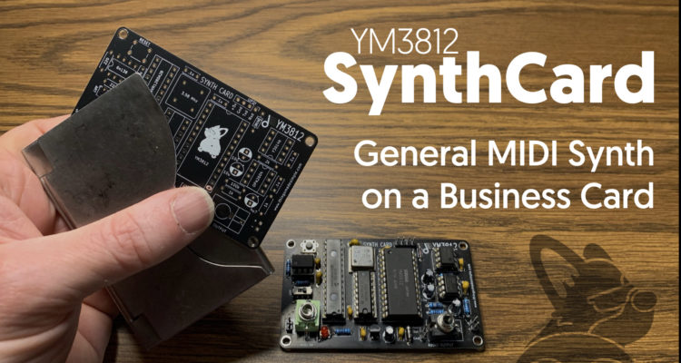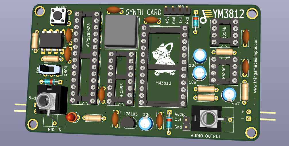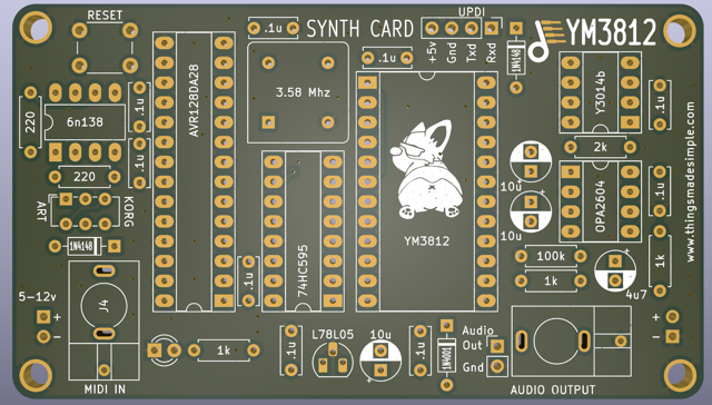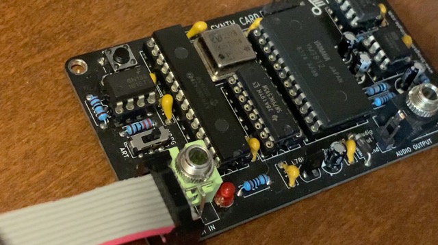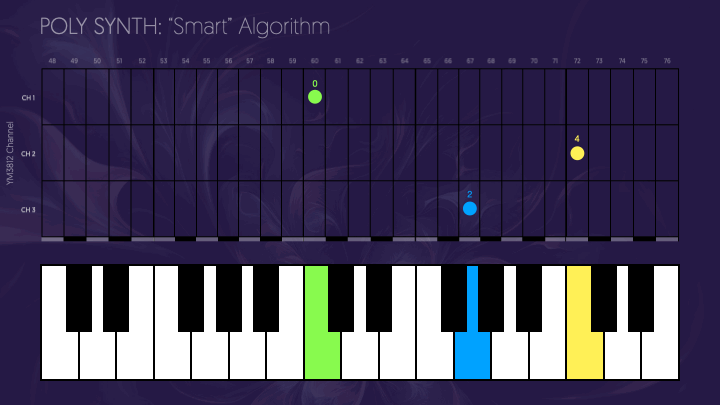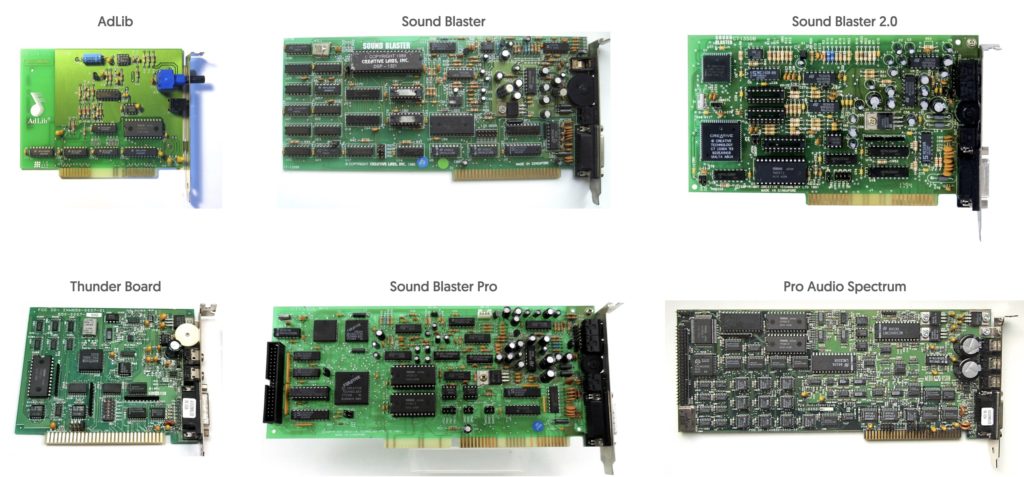

Over the last nine articles, we’ve covered lots of details on how to create a YM3812 OPL2 General MIDI synthesizer. We designed a basic hardware configuration and even crammed it into a business card sized PCB. Still, in most of these articles, I’ve focused far more on the software that controls the YM3812 than the hardware. The software holds most of the real complexity behind this module, and it felt unfair to just sweep it under the “check out my GitHub” rug. Don’t worry though, we will get to hardware again soon, but first we need to add one more software feature—pitch bend.
Pitch bend touches many areas of the code we’ve created so far, so I highly recommend reading some of the other articles (like Part 4 – MIDI Journey, Part 6 – Patches and Part 8 – Velocity Sensitivity) before jumping into this one. Those articles provide context for how I’ve structured the code, and why.
The Pitch Bend MIDI Events
To get things going, let’s start with how pitch bend information gets sent over MIDI. This information comes in the form of two variables: pitchBend and wheelNoteRange. The pitchBend variable indicates how far the user adjusted the pitch wheel, and the wheelNoteRange determines how many semitones the pitchBend value equates to. Both variables get communicated over MIDI, though in two very different ways.
pitchBend
MIDI communicates pitchBend through a Control Change event. Thankfully, the MIDI library handles the implementation for us and provides a separate handler call—similar to setHandleNoteOn:
MIDI.setHandlePitchBend(handlePitchBend)When called, the handlePitchBend function receives a 16-bit integer named pitchBend. This value ranges between 0x0000 and 0x3FFF, and describes how far the pitch wheel moved to the left or right. In order to map this to value to semitones, we need another variable called wheelRange.
wheelRange
This variable describes how many semitones the pitch wheel covers. By default, General MIDI assumes a range of 4 semitones. Using this range, a pitchBend value of 0x0000 maps to a note two semitones flat and a value of 0x3FFF maps to a note two semitones sharp. A value of 0x2000 sits right in the middle and equates to the original note.
Setting wheelRange requires a bit more doing because the “right” way to do it uses a MIDI RPN (Registered Parameter Number) command. Unfortunately our MIDI library does not support those commands, so I had to hack something together:
#define RPNMSB  101
#define RPNLSB  100
#define DATAMSB 6
#define DATALSB 38

uint16_t RPN_command = 0x7F7F;
void handleControlChange( byte channel, byte command, byte val ){
  switch( command ){
    case RPNMSB:  RPN_command = (RPN_command & 0x007F) | (val << 7);    break;
    case RPNLSB:  RPN_command = (RPN_command & 0xFF80) | val;           break;
    case DATAMSB: if( RPN_command==0 ) PROC_YM3812.setBendRange( val ); break;
    case DATALSB:                                                       break;
  }
}
RPN commands get delivered over a series of four control messages. Two of the messages communicate a 14-bit RPN command number, and the other two communicate a 14-bit data value.
Each RPN command triggers the handleControlChange function and passes a channel, command and value. Because an RPN command’s value requires 14 bits, the value gets broken up across two messages. One message contains the least significant 7 bits (RPNLSB) and the other contains the most significant 7 bits (RPNMSB). When received, these two messages override the appropriate bits in the RPN_command variable.
The least and most significant bits of the DATA value get communicated in the same way. Normally, we would combine the values associated with DATAMSB and DATALSB into a single value. But when it comes to the wheel range, these two values have different meanings. The MSB contains the number of semitones in the wheel range and the LSB contains a fractional number of semitones. We definitely don’t need that level of granularity and can thus ignore the LSB. Instead, when we receive the DATAMSB command we simply check if the RPN_command is zero and then call a function to set the bend range. And when we receive a DATALSB command, we just ignore it.
Convert pitchBend to Semitones
Cool, so now we know how far the pitch wheel moved (pitchBend) and the number of semitones that the pitch wheel covers (wheelNoteRange). How do we translate pitchBend into a number of semitones? Well, first we need to determine how many units of pitchBend equate to one semitone. I call this bendNoteSize:
This turns out to be pretty simple. We divide the constant PITCH_BEND_RANGE (0x3FFF) that represents the maximum value of pitchBend by the number of semitones in the wheel range. In the default General MIDI case where wheelNoteRange is 4, the bendNoteSize will be 0x1000.
The next thing we need to know is the maximum number of semitones that we can shift the pitch down. I call this bendNoteOffset:
With these two pieces in place, we can take a midi note and transpose it based on the value of pitchBend:
This formula takes a midi note, subtracts half of the wheel range and then adds back the number of semitones corresponding to the value of pitchBend. Now, if we isolate the right side of the formula and rearrange it, we get:
Where bend_note represents the number of whole semitones to add or subtract from a note in order to get the pitch-bent note. Of course pitch bend should have a far more granular response than just semitones. But because we are dealing with integers, dividing pitchBend by bendNoteSize will lose the fractional component. If we want to capture the remainder, we need one more formula:
This formula calculates the remainder of dividing pitchBend by bendNoteSize, telling us how close we are to the next note.
Mapping to FNums & Blocks
Now that we know how far we need to bend a pitch in terms of semitones and remainders of a semitone, let’s review how the YM3812 deals with frequencies.
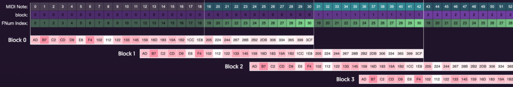
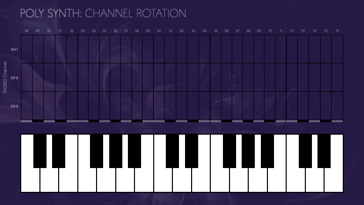
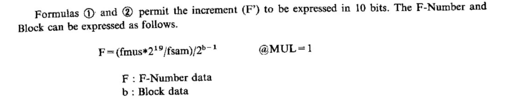
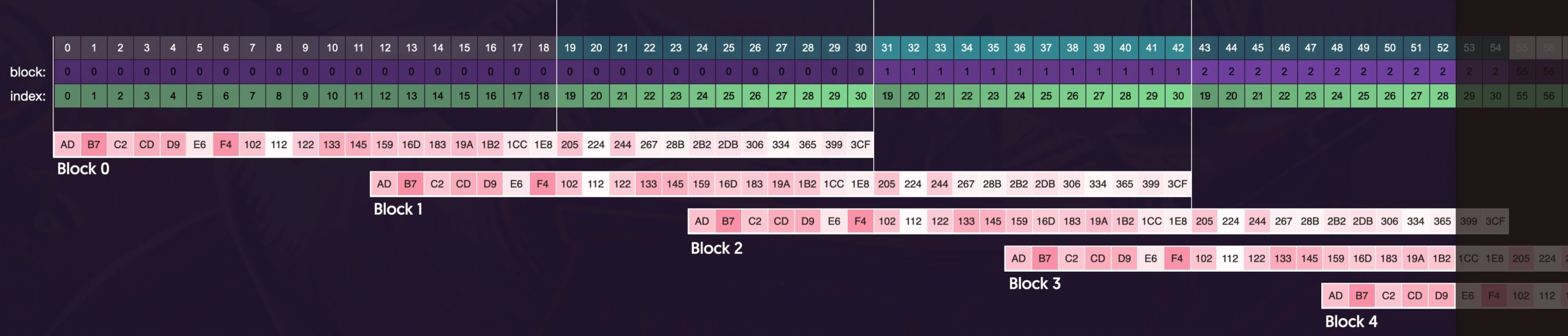
The YM3812 uses two different registers to determine the pitch of a note. Frequency Number translates a specific frequency into a relative frequency based on the chip’s 3.59 MHz clock. Back in article 4, we calculated a set of 30 FNums that map to the first 30 midi notes and stored them in a FREQ_SCALE array. Any notes higher than the 30th note require a value larger than the range that FNum can represent with 10 bits.
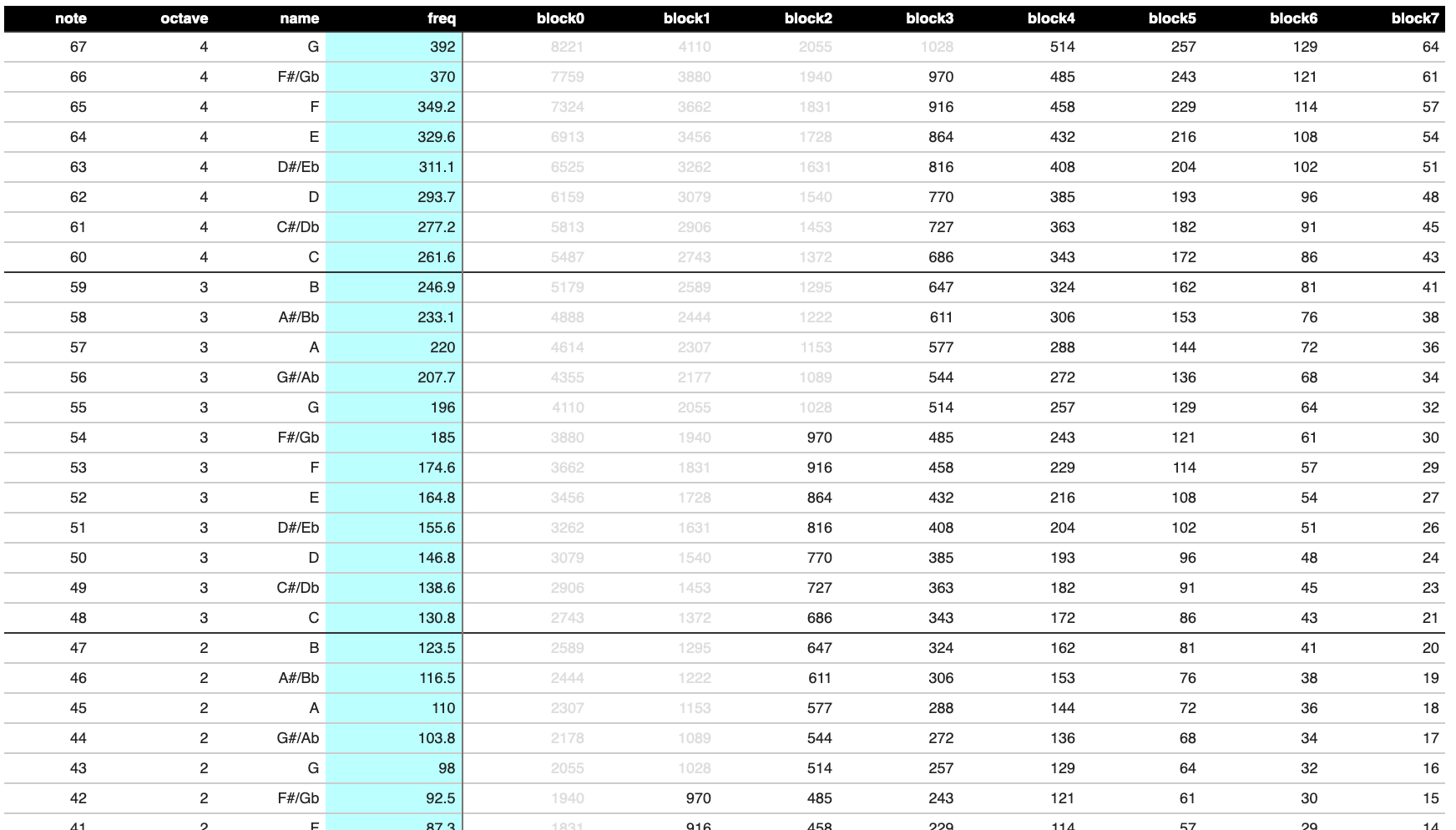
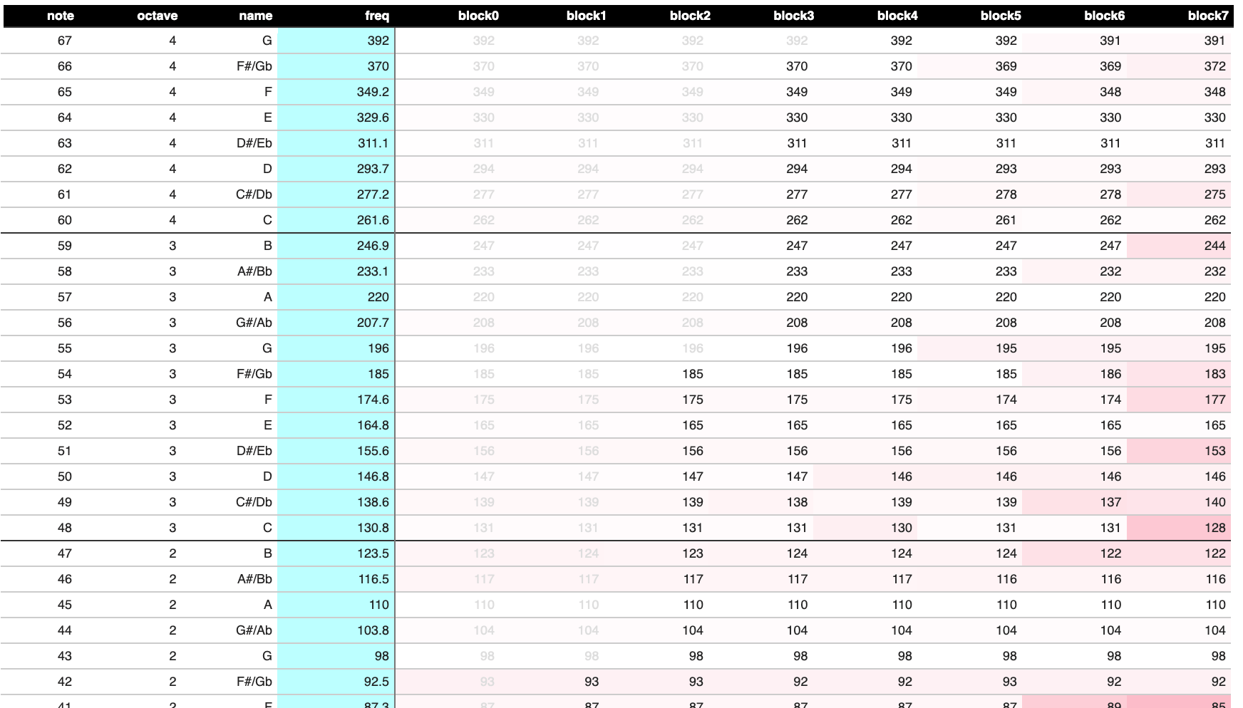
To work around this, the YM3812 uses a second register—Block—to adjust all of the FNums by some number of octaves. The image above shows how different midi notes map to different blocks and elements within our FRQ_SCALE array. Notice how many of the midi notes can be represented by multiple combinations of Block / FNum? To choose the best combination, we need to measure the accuracy of the resulting pitch. And that is indicated by the redness of each of the cells in the FREQ_SCALE. In general, the elements on the higher end of the scale will be the most accurate. So when we initially developed this, we chose to always use the top 12 elements and repeat them for all octaves.
Adding FNum Headroom
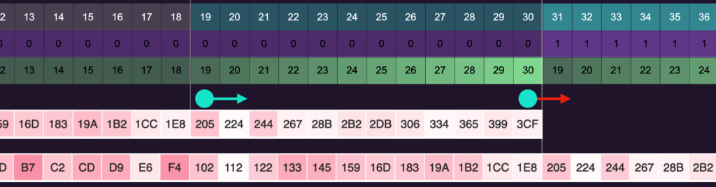
Zooming into the chart, we can start to see the challenge. To bend a pitch, we need to continuously interpolate between FNums. This means that we need an FNum for the current note and one for the next higher note on the scale. But if we are on MIDI note 30, there isn’t a higher FNum. To fix this, we need to shift the set of numbers that we repeat down by by one. Specifically, we need to repeat the frequency numbers 18 through 29 instead of 19 through 30. That way, we will always have a FNum available that is one higher than the current one. Here are the updated core formulas for determining the block and index of our FREQ_SCALE:
When the midi note number is 17 or lower, we use block 0 and the note number.
When the midi note number is 114 or higher, we can’t represent the note, so we have to ignore it.
For everything else in the middle:
One final thing here, the note that we feed into these formulas needs to include both the note we want to play and the number of semitones we want to bend. Hence, we first add bend_note onto midi_note before calculating the block and FNumIndex.
Interpolating Between Notes
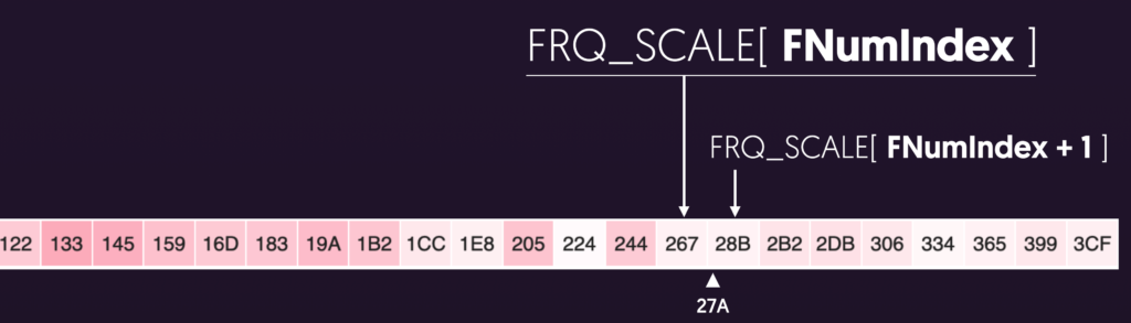
Now, with two guaranteed-valid FNums in hand, we just need to use bend_rem to interpolate between the lower and higher notes:
Here, FNumHigh refers to FRQ_SCALE[ FNumIndex+1] and FNumLow refers to FRQ_SCALE[ FNumIndex]. The formula takes the difference between the two notes and then adds a portion of that distance onto the lower FNum based on the percentage of bendNoteSize that bend_rem represents.
Lastly, because we are using integer math here, it’s critical that we divide by bendNoteSize AFTER multiplying the things on the top together:
That’s all the math. Let’s see how we build it!
Implementation Overview
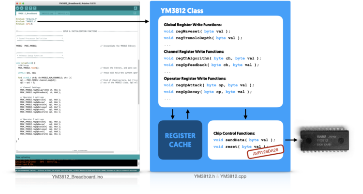
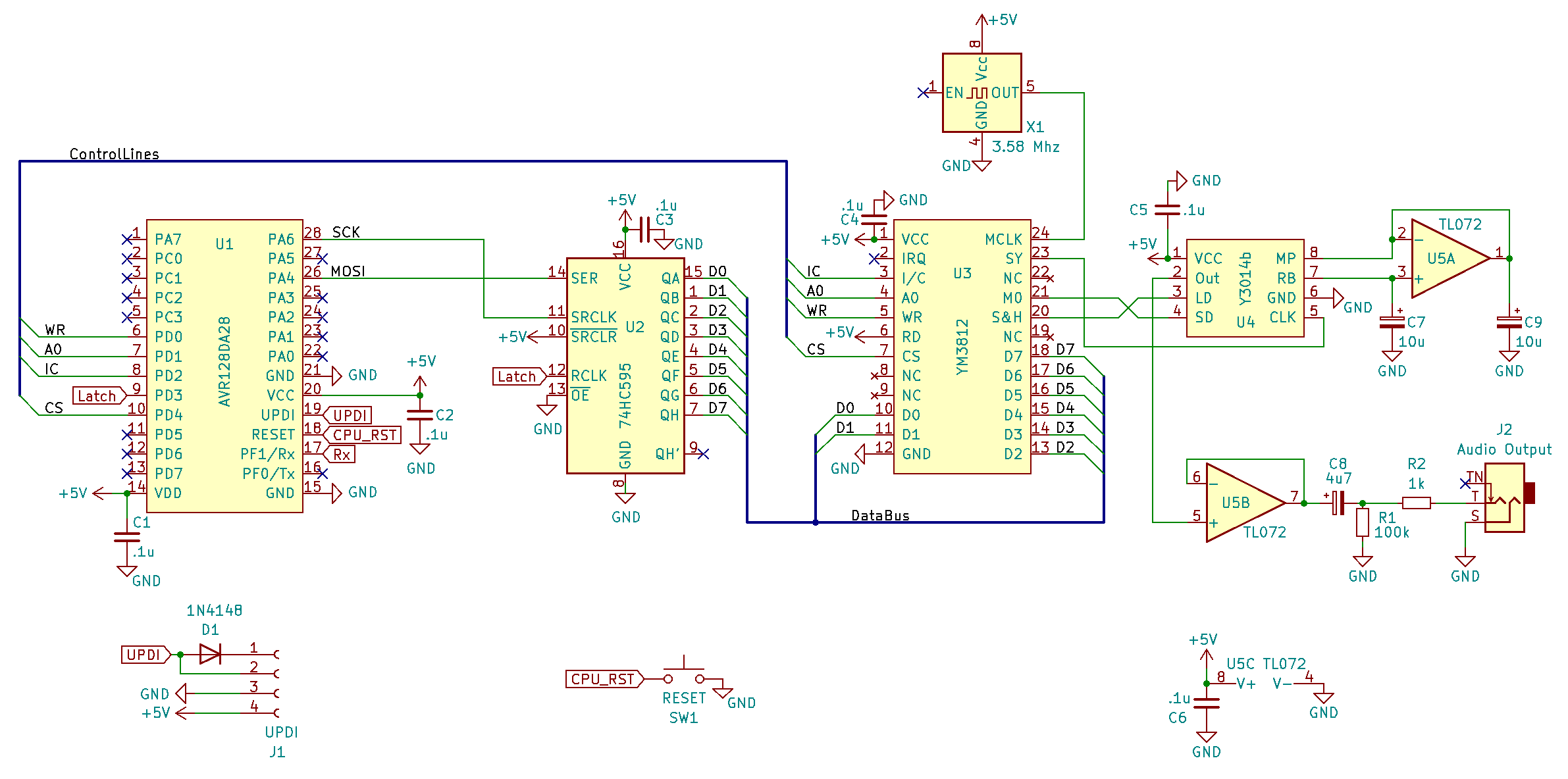
Now that we have a sense of how pitch bend works and the formulas involved, let’s take a look at how we can implement this into our code. This is the tenth article in the series, and we have quite a bit of code built out at this point. So to get oriented, let’s zoom out a bit and remember how things work today.
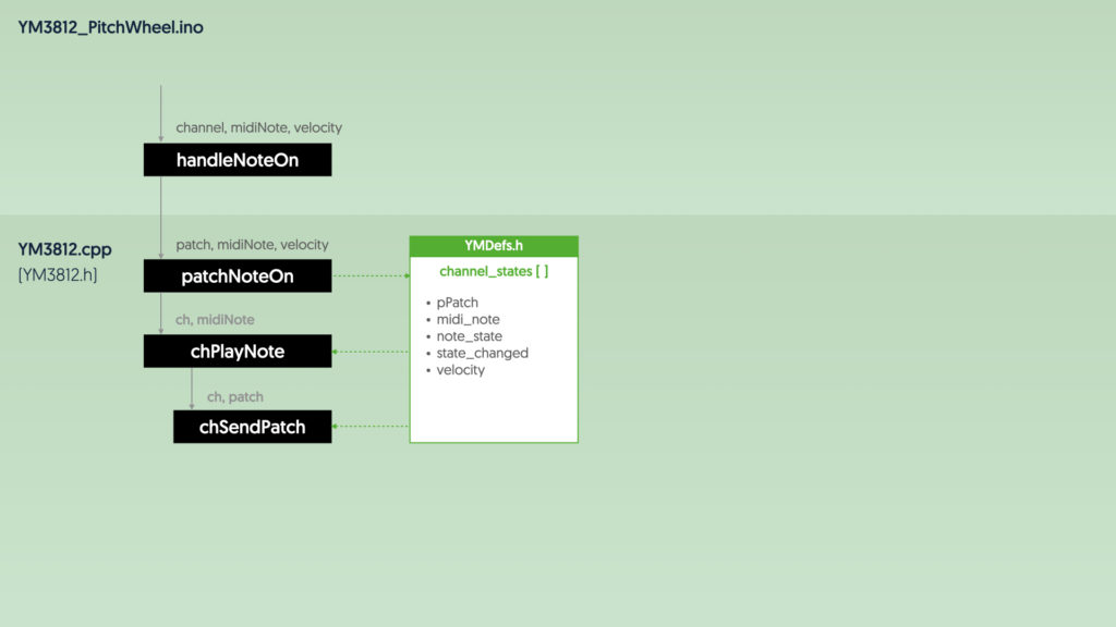
If you were to follow the flow for turning on a note, it would look something like this:
- The MIDI library calls the handleNoteOn function (in the .ino file)
- The handleNoteOn function calls patchNoteOn inside the YM3812 library and passes the patch, note and velocity
- patchNoteOn finds an open channel on the YM3812 and saves all relevant info into the channel_states array
- patchNoteOn calls chPlayNote and tells it which channel to use and which note to play
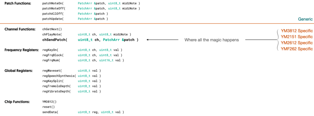
- chPlayNote calls chSendPatch to update the sound settings for the channel based on the patch
- chPlayNote calculates the frequency and sets the Block, FNum, and keyOn registers to play the note
Implementation Changes:
In order to implement pitch bend, we are going to have to changes a few things…
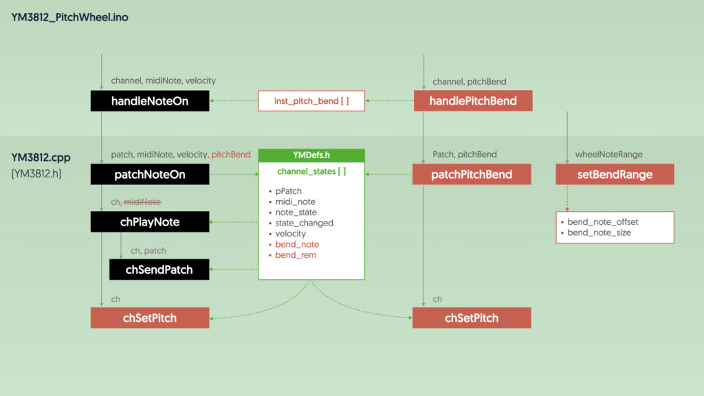
For now, let’s stay focused on the handle note flow. This works much the same way as it did before, but with a few tweaks. Let’s take those changes one by one.
handlePitchBend
The handlePitchBend function is new and gets called as soon as the user adjusts the pitch bend wheel. This function stores the new pitch bend value for the midi channel into the inst_pitch_bend array.
void handlePitchBend( byte channel, int16_t pitchBend ){
  uint8_t ch = channel-1;
  inst_pitch_bend[ch] = pitchBend + 0x2000;
  PROC_YM3812.patchPitchBend( inst_patch_data[ch], inst_pitch_bend[ch]);
}
The only quirk here is that the MIDI Library treats pitchBend as a signed integer that goes negative when the pitch wheel moves left and positive when the pitch wheel moves right. We add 0x2000 so that the value always stays positive and ranges from 0x0000 to 0x3FFF with a value of 0x2000 when centered.
This function also calls patchPitchBend to tell the YM3812 to update any currently playing notes with the new pitch bend value. We still need to write that function, and will come back to it in a bit.
handleNoteOn
With the current value of pitchBend captured, we can now pass that on in our handleNoteOn function:
void handleNoteOn( byte channel, byte midiNote, byte velocity ){
  uint8_t ch = channel - 1;
  uint8_t drumIndex;

  if( DRUM_CHANNEL == channel ){
    drumIndex = (midiNote - FIRST_DRUM_NOTE) % NUM_DRUMS;
    PROC_YM3812.patchNoteOn( drum_patch_data[drumIndex], velocity );
  } else {
    PROC_YM3812.patchNoteOn( inst_patch_data[ch], midiNote, velocity, inst_pitch_bend[ch]);
  }

}
Nearly everything in this function remained the same as before. But if you look at the last line, we now pass the value of inst_pitch_bend associated with the MIDI channel playing the note. Note that we don’t do this for drums, just for melodic instruments.
patchNoteOn
Now let’s see what the YM3812 library does with the pitchBend information.
void YM3812::patchNoteOn( PatchArr &patch, uint8_t midiNote, uint8_t velocity, uint16_t pitchBend ){
  last_channel = chGetNext();
  channel_states[ last_channel ].pPatch  = &patch;
  channel_states[ last_channel ].midi_note  = midiNote;
  channel_states[ last_channel ].velocity = velocity;
  channel_states[ last_channel ].note_state = true;
  channel_states[ last_channel ].state_changed = millis();

  if( pitchBend == 0x2000 ){
    channel_states[ last_channel ].bend_note = 0;
    channel_states[ last_channel ].bend_rem = 0;
  } else {
    channel_states[ last_channel ].bend_note = (pitchBend / bend_note_size) - bend_note_offset;
    channel_states[ last_channel ].bend_rem = pitchBend % bend_note_size;
  }

  chPlayNote( last_channel );
}
This function selects a YM3812 channel to use and then saves all of the state information about that channel into the channel_states array. Most of this function stays the same, but now we need to calculate and save values for bend_rem and bend_note. There are two cases. In the easy (and most likely) case, the user has not adjusted the pitch wheel and we can directly set bend_note and bend_rem to zero.
In the other case, the user HAS adjusted the pitch wheel and we need to calculate values for bend_rem and bend_note using the formulas we identified earlier in the article. These formulas depend on two other variables bend_note_size and bend_note_offset. For efficiency reasons, we calculate these values only once when setting the wheel note range. Let’s have a look:
setBendRange
void YM3812::setBendRange(uint8_t wheelNoteRange){
  if( wheelNoteRange < 2 ) return;
  bend_note_offset = wheelNoteRange >> 1;
  bend_note_size   = PITCH_WHEEL_RANGE / (wheelNoteRange & 0xFFFE);
}
This function takes the number of notes that the pitch wheel maps to and updates bend_note_offset and bend_note_size accordingly. This function also enforces a couple of critical constraints. First, the wheel range has to be even. For example if the wheelNoteRange is 2, then the pitch wheel goes from -1 semitone to +1 semitone. That works great. But if you set wheelNoteRange to 3, then the pitch wheel would go from -1.5 semitones to +1.5 semitones and that would be much harder to implement (and explain).
To enforce this rule, I logically AND wheelNoteRange with 0b1111111111111110 (0xFFFE). This ensures the last bit is always zero and thus the number is always even. This also creates a potential issue. If wheelNoteRange is less than 2, then the result will always be zero. And if the range is zero, then dividing by that range produces undesirable affects. So, the first line of code just ignores attempts to set the value to less than 2.
chPlayNote
After setting bend_note and bend_rem, the patchNoteOn function calls chPlayNote. I changed this function quite a bit.
void YM3812::chPlayNote( uint8_t ch ){
  regKeyOn( ch, 0 );
  chSendPatch( ch, *channel_states[ch].pPatch );
  chSetPitch( ch );
  regKeyOn( ch, 1 );
}
The first key change is that the function only accepts one argument instead of two. I removed midiNote as argument. Why? Well, midiNote has always been stored inside of the channel_states array, so, technically we’ve never actually needed to pass it directly to the function. This became more apparent when, in addition to midi_note affecting the pitch, we now have bend_note and bend_rem that ALSO affect the pitch. Rather than pass all three variables around, I kept things simple.
There’s something else that looks simpler about this function… All of the code that sets the pitch has been replaced with a call to a new function, chSetPitch.
chSetPitch
I added the chSetPitch function because there are now two cases where the user needs to adjust the pitch: when turning on a note, and when adjusting the pitch bend. Having a separate chSetPitch function keeps things nice and tidy.
void YM3812::chSetPitch( uint8_t ch ){
  uint8_t block, fNumIndex;
  uint8_t midiNote = channel_states[ch].midi_note+channel_states[ch].bend_note;

  if( midiNote > 127 ) midiNote = 0;
  if( midiNote > 113 ) return;

  if( midiNote < 18 ){
    block = 0;
    fNumIndex = midiNote;
  } else {
    block = (midiNote - 18) / 12;
    fNumIndex = ((midiNote - 18) % 12) + 18;
  }

  uint16_t lFNum = FRQ_SCALE[fNumIndex];
  uint16_t hFNum = FRQ_SCALE[fNumIndex+1];
  uint16_t FNum = (uint32_t(hFNum - lFNum) * uint32_t(channel_states[ch].bend_rem)) / bend_note_size + lFNum;

  regFrqBlock( ch, block );
  regFrqFnum(  ch, FNum  );
}
Much of this code lived in the chPlayNote function previously, so it may look familiar. But let’s go through it. First, we decide which note we want to play. This is based on both the midi_note that the user played as well as the whole number of semitones to bend the note—bend_note. We add these two values together and get a new midiNote to use.
In the next section, we use this new midiNote to calculate the block number and index into the FREQ_SCALE array—fNumIndex. This code is identical to what was in chPlayNote, but the ranges have been altered by one. So, as we discussed earlier in the article, 114 became 113, and 19 became 18. This ensures that fNumIndex+1 will always be a valid index in the FREQ_SCALE array.
The next three lines of code interpolate between the current note and the next note based on the bend_rem. One small nuance here is that we need to cast things as a 32-bit integers before multiplying them. Otherwise we will overflow a 16-bit number which will lead to some unexpected results. Once we divide that result by bend_note_size, the value will be small enough to fit back into a 16 bit integer, so FNum can still be a uint16_t.
With FNum calculated, we use our two register functions to upload it along with block to the YM3812.
You did it! You’ve uploaded a pitch-bent note to the YM3812! But wait… there’s more!
patchPitchBend
Back when we were looking at the handlePitchBend function, I said I would come back to this line of code here:
PROC_YM3812.patchPitchBend( inst_patch_data[ch], inst_pitch_bend[ch]);
Well, it’s time! See there are really two different use-cases we need to handle with pitch bend. In the first case, the user moves the pitch bend wheel and then plays a note. That’s what we have implemented so far. But in the second (and more likely case) the user plays a note and THEN moves the pitch wheel. That is the case that the patchPitchBend function accommodates.
In order to pull this off, we need to know which of the notes currently playing on the YM3812 associate with the MIDI channel that sent the pitch bend command. Thankfully, our channel_states array contains a pointer to the patch for each active note, and we can use that to decide which YM3812 channels to update. This is why, in addition to the pitchBend argument, we also pass a pointer to the patch associated with the MIDI channel.
Here is how it works:
void YM3812::patchPitchBend( PatchArr &patch, uint16_t pitchBend){
  for( byte ch = 0; ch < num_channels; ch++ ){
    if( channel_states[ch].pPatch == &patch ){

      if( pitchBend == 0x2000 ){
        channel_states[ ch ].bend_note = 0;
        channel_states[ ch ].bend_rem = 0;
      } else {
        channel_states[ ch ].bend_note = (pitchBend / bend_note_size) - bend_note_offset;
        channel_states[ ch ].bend_rem = pitchBend % bend_note_size;
      }

      chSetPitch(ch);
    }
  }
}
The function first loops through every channel in the channel_states array to see whether it is associated with the patch passed to the function. If it is, then the middle portion of the code updates the values of bend_note and bend_rem based on the value of pitchBend. If this code looks familiar, that’s because it’s identical to the code we added to the patchNoteOn function.
Finally, after updating things in the channel_states array, we call chSetPitch to calculate and update the frequency registers on the YM3812.
Conclusion & Links
Well, that about wraps up how you affect pitch bend on a YM3812. Possible? Totally. Difficult to implement? A bit… Hard to explain? Oh my goodness, yes. So, if anything didn’t make sense please let me know in the comments!
As always, the code is available on GitHub. If you give it a shot, let me know how it goes!
As for the next article, I’d like to go back to the breadboard and add another YM3812 for true stereo output. We should be able to take advantage of Velocity Sensitivity and Pitch Bend to create Stereo Panning and Detuning, and I think that would be pretty cool. What do you think?
See you next time!